5.3 Layout Phase
Table of contents
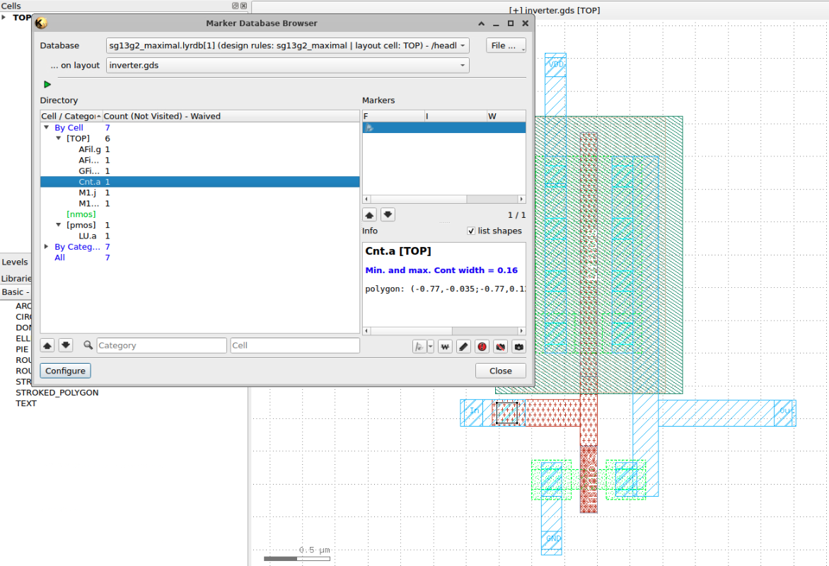
Creating the physical layout of the CMOS inverter is essential for fabrication and further analysis process. In this section, we are going to do layout designing and DRC handling, spice generation of layout and LVS checking using NETGEN.
Prerequisites
- KLayout
- IHP SG13G2 PDK klayout technology library
- If not locally installing KLayout, you can also use IIC-OSIC-TOOLS with KLayout and sg13g2 tech libraries pre-installed (Recommended for MAC users).
KLayout Setup Steps
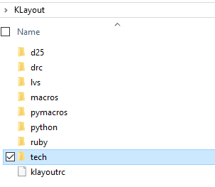
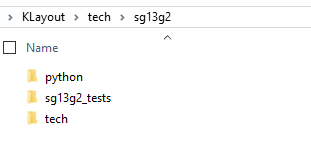
We start with installing KLayout (if you are using a Windows PC) and opening the KLayout technology folder. In windows, this folder is usually located in C:\Users\<username>\KLayout and looks as shown below. If a folder called tech is missing inside the KLayout folder, you may create this folder yourself.
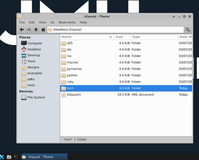
In IIC-OSIC-TOOLS, you will find the .klayout folder inside /headless/.klayout/ as shown below. You may have to create the folder tech yourself. This tech folder is where we store all KLayout technology libraries. Hence, you need another folder called sg13g2 inside tech to store the IHP SG13G2 technology libraries. These libraries are stored in the github repository: ihp-sg13g2/libs.tech/klayout.
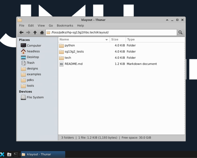
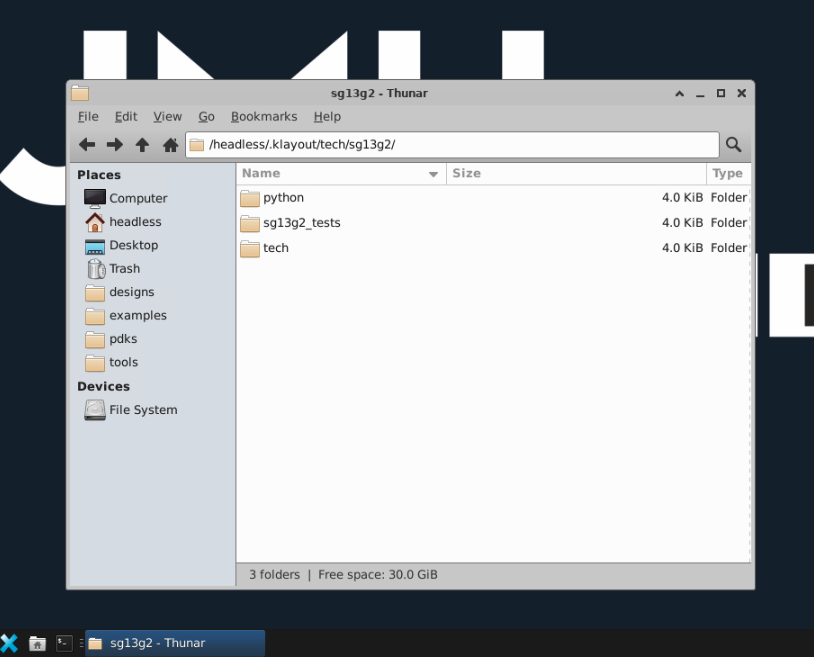
In IIC-OSIC-TOOLS, you can find the technology libraries inside /foss/pdks/ihp-sg13g2/libs.tech/klayout/, which you can copy and paste inside /headless/.klayout/tech/sg13g2 as shown below.
For Windows, you can download them from the github repository: ihp-sg13g2/libs.tech/klayout and copy and paste inside \KLayout\tech\sg13g2\ as shown below.
The most important technology files are inside the \KLayout\tech\sg13g2\tech folder as shown below.
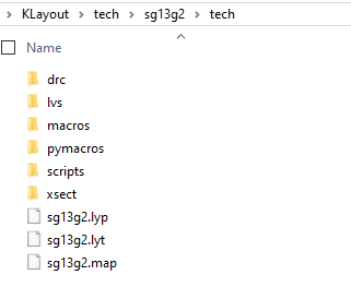
📁 Directory: KLayout > tech > sg13g2 > tech
📄 Files
| File Name | Type | Description |
|---|---|---|
sg13g2.lyp |
Layer Properties File | Defines how layers are displayed in KLayout (colors, patterns, visibility). |
sg13g2.lyt |
Layout Technology File | Contains technology-specific settings like layer mappings and design rules. |
sg13g2.map |
Layer Mapping File | Maps layer numbers/names between different formats or tools. |
📁 Folders
| Folder Name | Likely Contents / Purpose |
|---|---|
drc |
Design Rule Check scripts or configuration files. |
lvs |
Layout Versus Schematic rule files for verifying layout against circuit schematics. |
macros |
KLayout macros, possibly in Ruby or another supported scripting language. |
pymacros |
Python-based macros for automating tasks in KLayout. |
scripts |
General-purpose scripts, possibly for setup, automation, or utilities. |
xsect |
Likely contains cross-section related data or visualization scripts. |
The next important folder is the \KLayout\tech\sg13g2\python, which contains the following 3 folders:
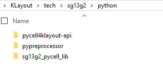
The pypreprocessor and the pycell4klayout-api are both empty folders, if you downloaded the technology files from github (not in IIC-OSIC-TOOLS). Download these files from the links given below and put them inside the folders.
pycell4klayout-api: https://github.com/IHP-GmbH/pycell4klayout-api/tree/047f1928ac6749d438a500c4ee90f32c879d3f11pypreprocessor: https://github.com/IHP-GmbH/pypreprocessor/tree/6ddd5783365718c41eb69bce4428358ace4d1fa2
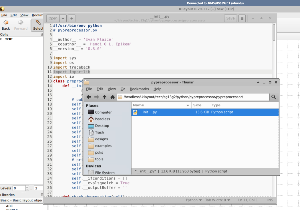
Python 3.12 error - “No module names imp”
If you encounter an error such as above for imp module, then you can find details on how to fix it here.
This error usually comes from the _init_.py file of /headless/.klayout/tech/sg13g2/python/pypreprocessor/pypreprocessor/_init_.py as shown below. Repacing this file with the version here may also work.
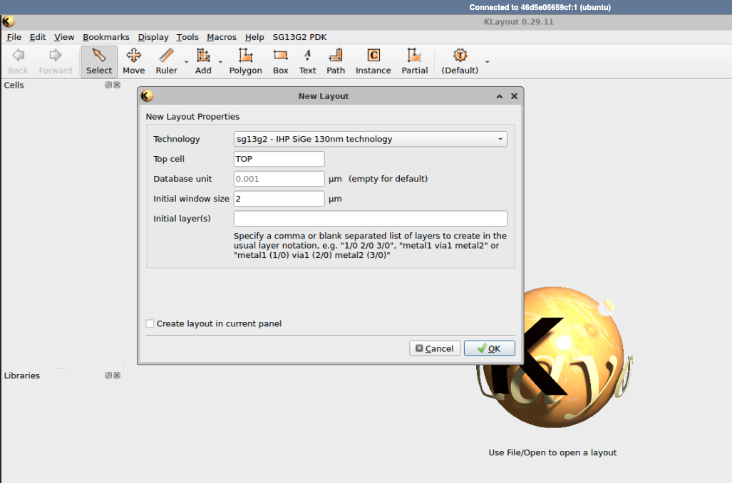
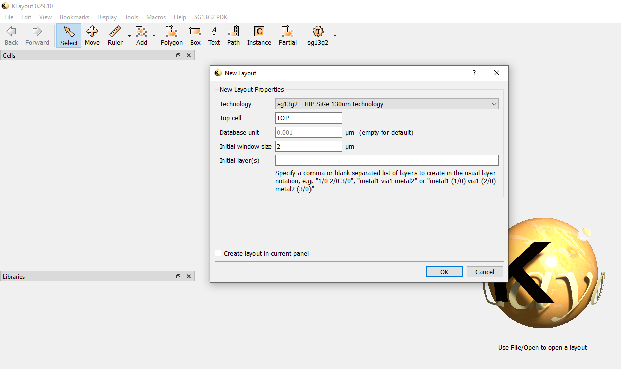
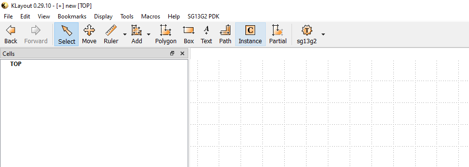
Now we can start by opening the KLayout (Editor) application. In the terminal, you can use the command klayout -e comand to open it. Go to File>>New Layout and create a new layout as shown below. Choose sg13g2 as the technologyand name the top cell as “TOP”.
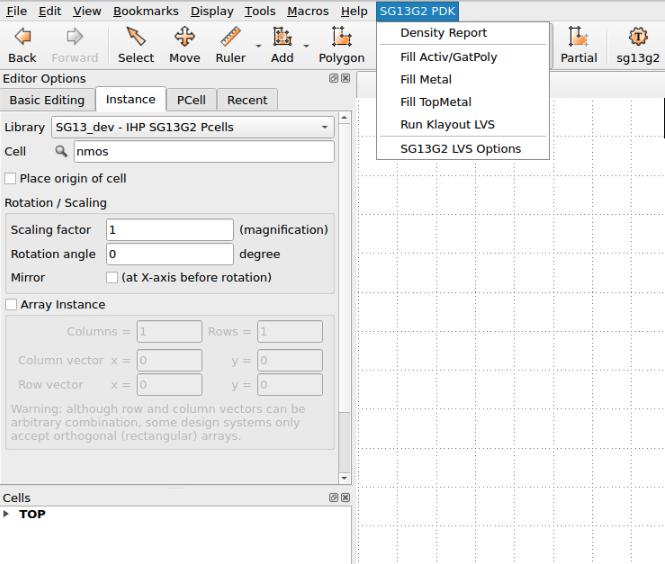
If you can see the tab SG13G2 PDK in the Menu Bar, then everything has been installed correctly.
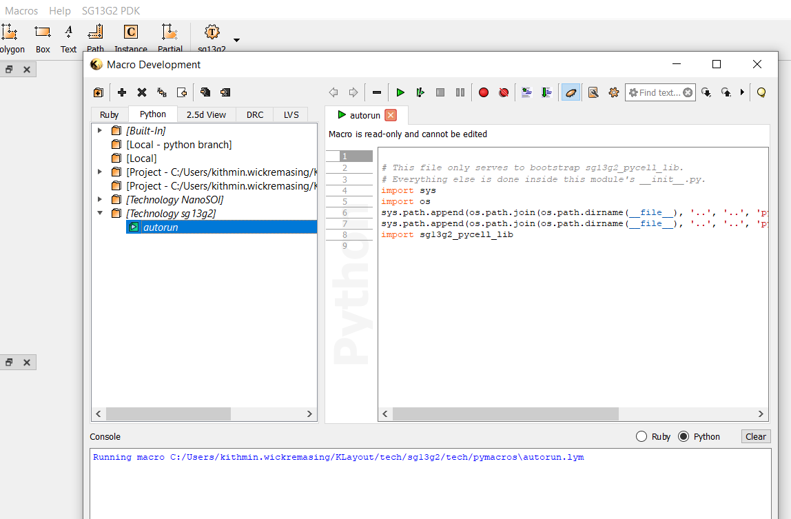
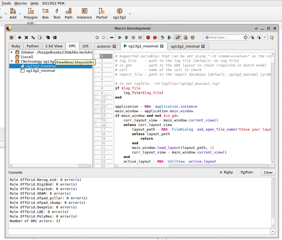
In order to ensure that, you cn go to Macros»Macro Development and then go to the Python tab and then double-click on the autorun script. You can run this script by clicking the green rectangle. If this script is able to run without any errors as shown below, then you are good to proceed to the next stage.
Structure of the CMOS Inverter
Before moving into layout design we have to get some idea about the physical structure of a CMOS transistor in Silicon level. This is the schematic design of the inverter.
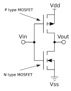
Figure: The CMOS inverter
It consists of a P-type MOSFET and a N-type MOSFET, and includes key structures like diffusion areas, gate oxides, polysilicon gates, metal layers and vias etc.

Figure: The CMOS inverter layout side-view
- Active Area (Diffusion): Regions where transistors are formed. These areas are doped to create n-type or p-type regions.
- Gate Oxide: A thin layer of SiO₂ between the gate and the channel region of the transistor.
- Polysilicon Gate: The gate electrode controlling the transistor’s operation, formed above the gate oxide.
- Contacts and Vias: Metal connections that link the transistors to interconnect layers and power supply.
- Metal Layers: Conductive layers (e.g., metal1, metal2) used for interconnections between different components.
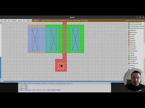
Layout Design Steps
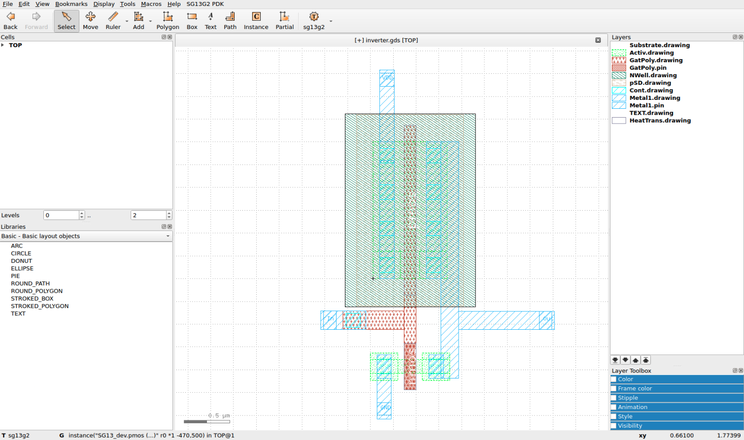
This is how you connect the PMOS (top) and NMOS (bottom) transistor cells together in your layout, and also connect the VDD and GND power rails to create the inverter layout. The “In” and “Out” labels indicate the INPUT and OUTPUT ports of the inverter.
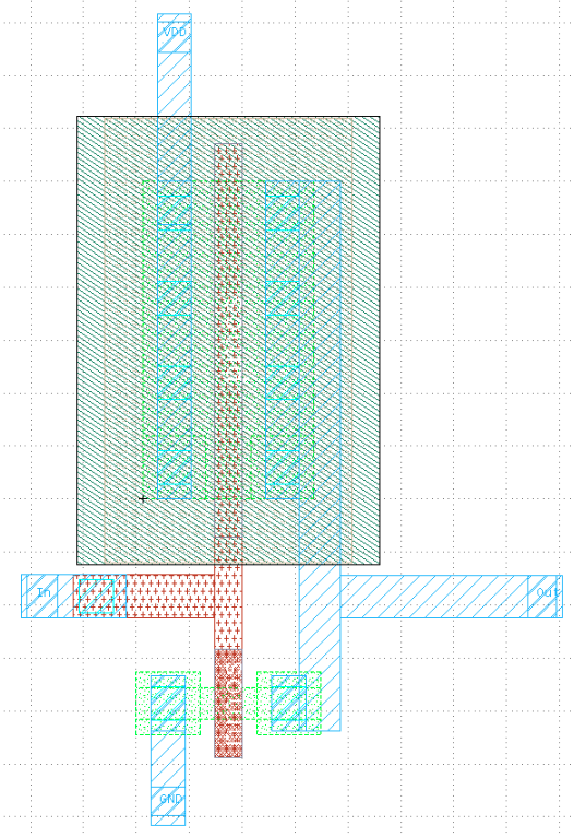
Figure: CMOS inverter design in IHP SG13G2 using Klayout
How do we go about building this layout in KLayout (or Magic)?
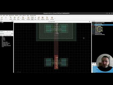
Step 2a - Inverter Layout in Magic for IHP SG13G2 130nm PDK
Step 2b - Inverter Layout in KLayout for IHP SG13G2 130nm PDK
The GDSII file of the inverter can be found here and the GDSII files of all the P-cells can be found here.
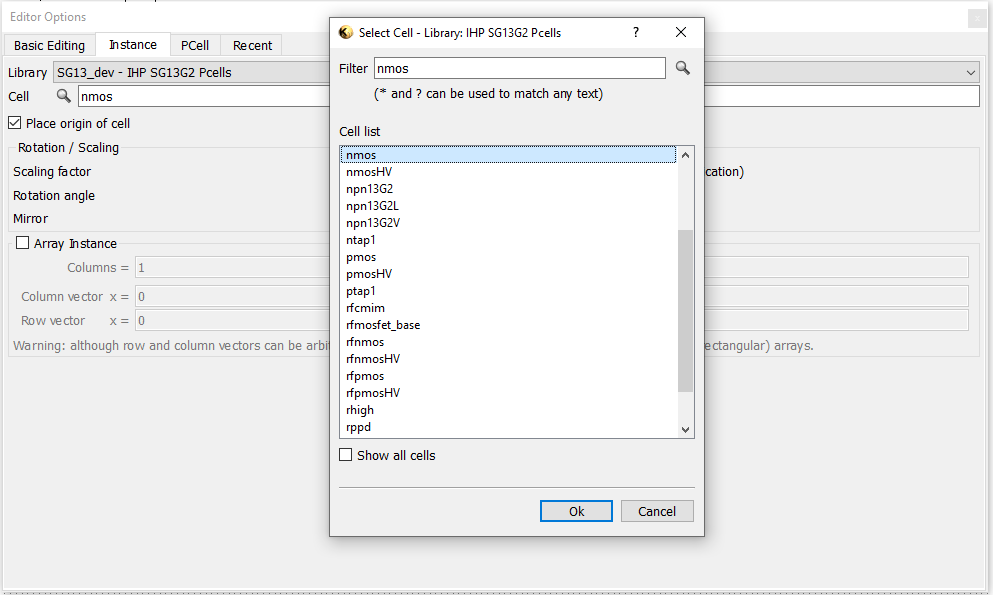
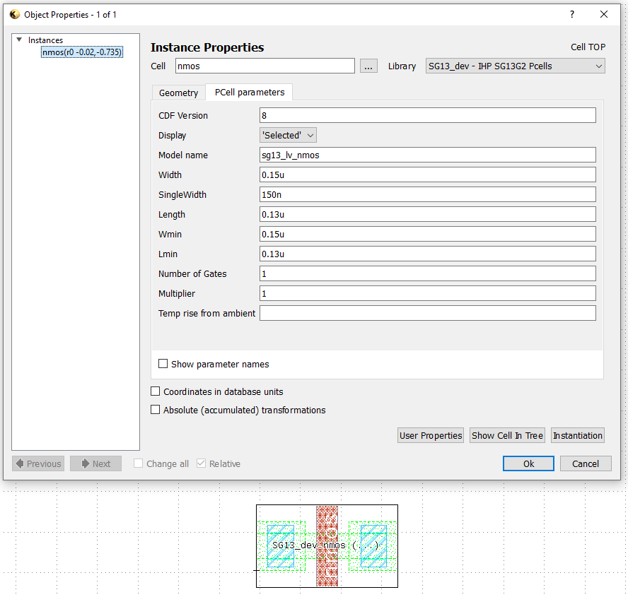
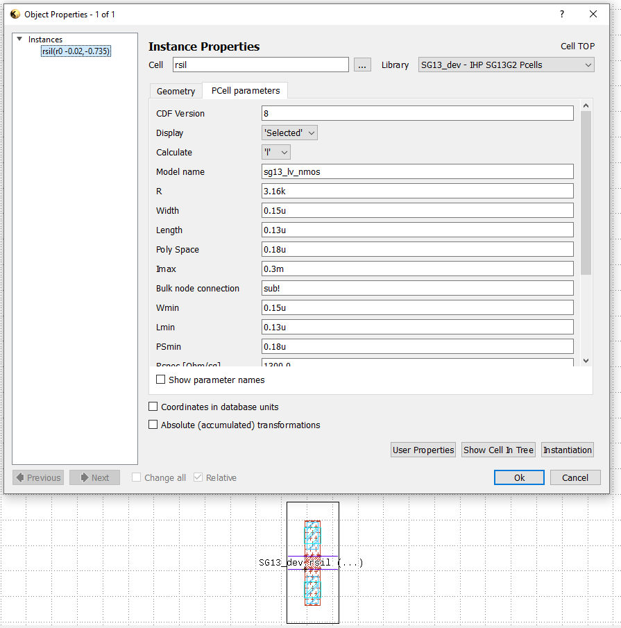
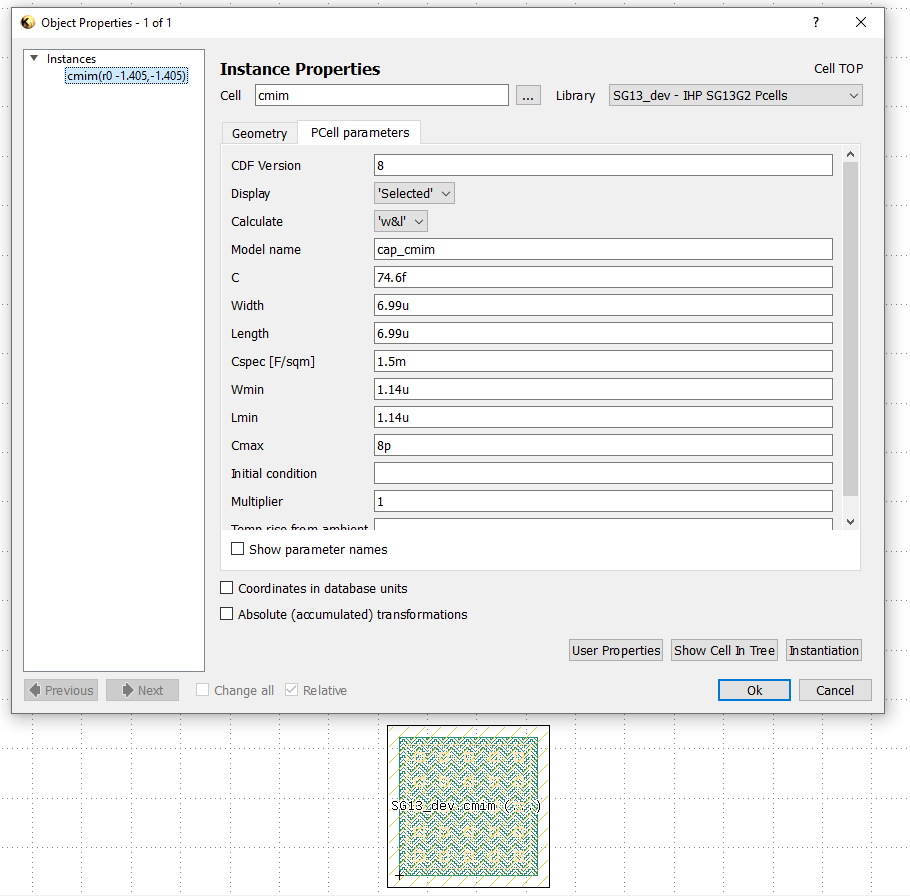
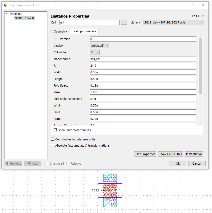
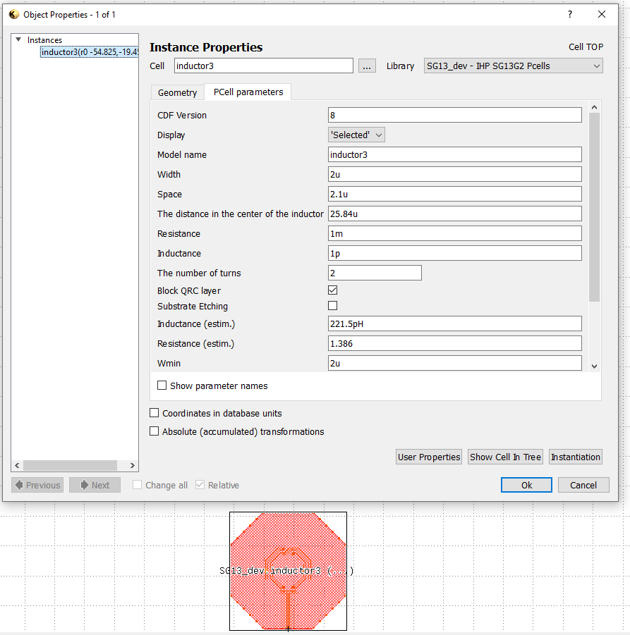
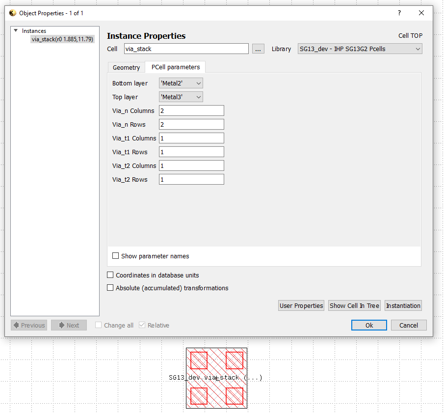
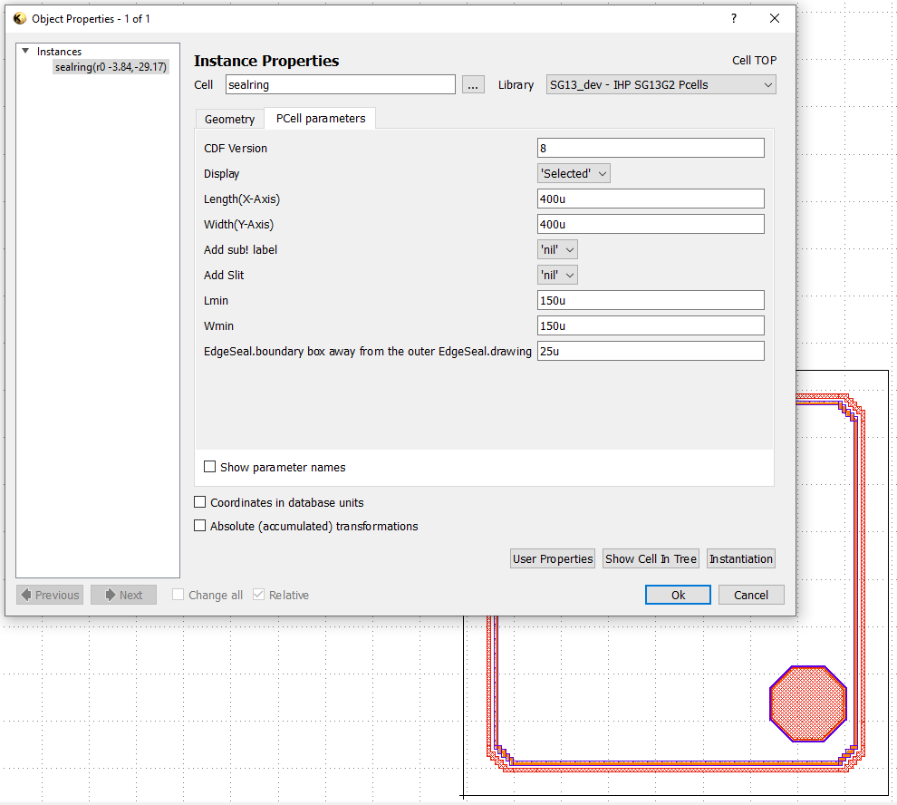
P-Cells
Extra sections with more information:
- https://github.com/IHP-GmbH/IHP-Open-PDK/tree/main/ihp-sg13g2/libs.tech/klayout/tech/lvs
- https://github.com/IHP-GmbH/IHP-Open-PDK/tree/main/ihp-sg13g2/libs.tech/klayout/tech/xsect
3D Layout
Can you identify the P and N type MOSFETs? Can you see the input and output ports? Here’s a 3D view of the same cell:
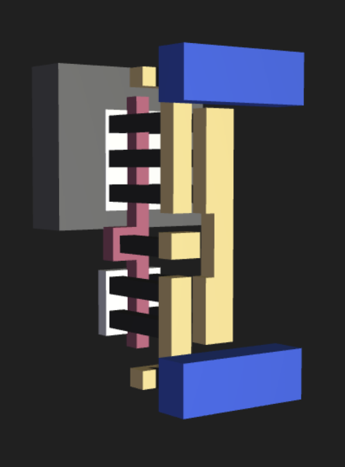
Figure: CMOS inverter 3D design
Learning to draw a CMOS inverter?
For more information, refer to these tiny tapeout resources.
Design and Layout Rules
You can find information about the DRC rules in the document below, which is available for download here.