4.2 IHP’s SG13G2 MOSFETs
Table of contents
MOSFET Types and Symbols
The SG13G2 PDK provides parameterizable MOSFET symbols in Xschem:
- Low-Voltage MOSFETs (1.5 V)
sg13_lv_nmos: \(V_{th}\) ~ 0.5 V, \(L_{min}\) = 0.13 µmsg13_lv_pmos: \(V_{th}\) ~ -0.47 V, \(L_{min}\) = 0.13 µm
- High-Voltage MOSFETs (3.3 V)
sg13_hv_nmos: \(V_{th}\) ~ 0.7 V, \(L_{min}\) = 0.45 µmsg13_hv_pmos: \(V_{th}\) ~ -0.65 V, \(L_{min}\) = 0.45 µm
Symbols support the configuration of width (W), length (L), and multiplier (m). Isolated variants of NMOS are also available.
What is an Isolated NMOS?
In standard CMOS, all NMOS devices share a common P-substrate, meaning they share the body terminal.
An isolated NMOS:
- Is fabricated inside a deep N-well embedded in a P-type epitaxial layer.
- This allows the body terminal to be independently biased.
- Provides true 4-terminal operation (G, D, S, B).
Benefits of Isolated NMOS
- Independent body control
- Reduced parasitic coupling
- Mitigates latch-up
- Improves analog and RF performance
CMOS Transistor Terminals (4-pin mode)
| Terminal | Symbol | Function |
|---|---|---|
| Gate | G | Controls the channel (via voltage) |
| Drain | D | Where current exits the transistor |
| Source | S | Where current enters the transistor |
| Body | B | Substrate; influences threshold voltage and leakage |
The Role of the Body Terminal
- The body terminal in an NMOS is typically connected to the lowest voltage (GND).
- This prevents the body effect, which increases the threshold voltage \(V_{th}\) if the source and body are not at the same potential.
- The body terminal also helps prevent leakage and latch-up issues.
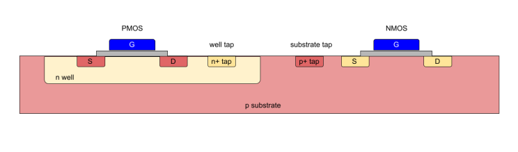
Figure : CMOS using normal process(not isolated)
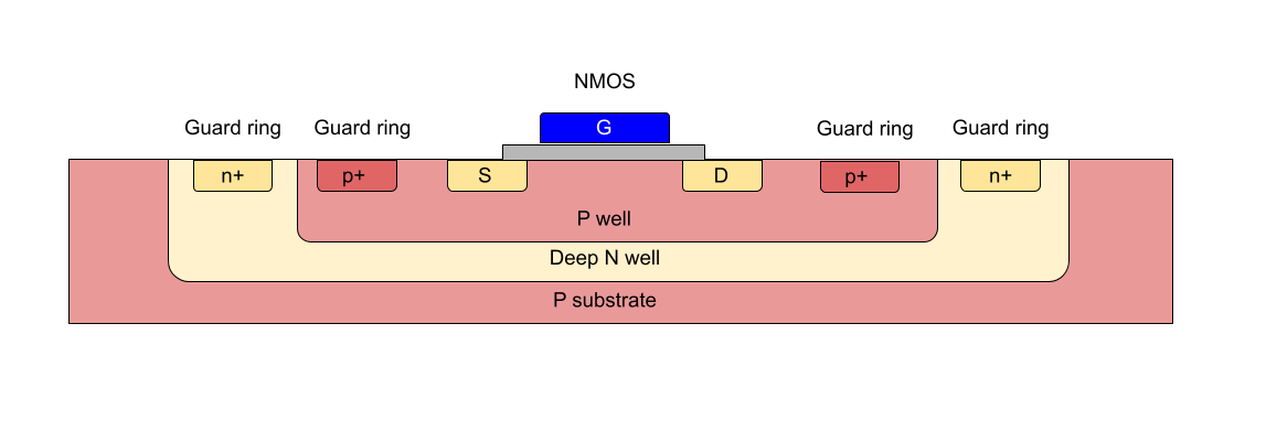
Figure : Isolated NMOS
MOSFET analysis for analog design
A Metal-Oxide-Semiconductor Field-Effect Transistor (MOSFET) is a voltage-controlled semiconductor device widely used in analog and digital circuits. In analog design, MOSFETs are crucial for building amplifiers, filters, current mirrors, bias circuits, and operational transconductance amplifiers (OTAs).
- Four-terminal structure: Gate (G), Drain (D), Source (S), Bulk/Substrate (B)
Types of MOSFETs
- NMOS: Conducts when \(V_{GS}\) > \(V_{th}\) , uses electrons as carriers (higher mobility).
- PMOS: Conducts when \(V_{SG}\) > \(\|V_{th}\|\) , uses holes as carriers (lower mobility).
NMOS vs. PMOS
NMOS is preferred for speed; PMOS complements NMOS in CMOS logic for power efficiency.
MOSFET as a Voltage-Controlled Current Source
The MOSFET allows current to flow from drain to source, controlled by the gate voltage.
In saturation, the drain current is mainly controlled by VGS:
Why Use MOSFETs in Analog Design?
- Low input current due to insulated gate (nearly zero gate current).
- Scalability and high integration in CMOS processes.
- Design flexibility: Can act as resistors, current sources, amplifiers, and switches.
- Matching and noise performance for precision analog blocks.
MOSFET Symbols and Conventions
| Symbol Type | Description |
|---|---|
| Enhancement-mode | Most common in CMOS (normally OFF) |
| Depletion-mode | Less common (normally ON) |
| 4-Terminal | Gate, drain, source, and bulk |
| 3-Terminal | Bulk tied to source (simplified view) |
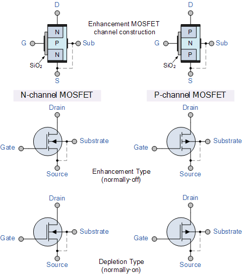
Figure : MOSFET symbols for each
DC Characteristics (Ideal Behavior)
| Region | Condition | Behavior |
|---|---|---|
| Cutoff | \(V_{GS} < V_{th}\) | MOSFET is OFF, \(I_D = 0\) |
| Triode | \(V_{GS} > V_{th}\), \(V_{DS} < V_{GS} - V_{th}\) | MOSFET behaves like a resistor |
| Saturation | \(V_{GS} > V_{th}\), \(V_{DS} \geq V_{GS} - V_{th}\) | Current saturates, good for amplifiers |
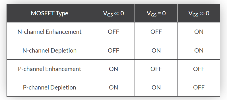
Figure : Switching characteristics of both the N-channel and P-channel type MOSFET.
Now, in the next section we will continue to analyse the characteristics of a MOSFET.