2.5 The Bipolar Junction Transistor (BJT)
A Bipolar Junction Transistor (BJT) is a three-terminal active semiconductor device used to amplify or switch electronic signals. It consists of two p-n junctions configured in either NPN or PNP formation. Current flowing into one terminal (the base) controls the current flowing between the other two terminals (collector and emitter), making it a current-controlled device.
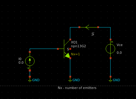
The following circuit shows a BJT in a common-emitter configuration. The xschem simulation file can be found here.
Characteristics
BJT operation is governed by the relationship between the base-emitter and collector-emitter voltages. In the active region, the collector current \(I_C\) is given by:
\[I_C = \beta I_B\]where:
- \(I_C\) is the collector current,
- \(I_B\) is the base current,
- \(\beta\)(or \(h_{FE}\)) is the DC current gain of the transistor.
BJTs have three operating regions:
- Cut-off: Both junctions reverse biased → transistor OFF
- Active: Base-emitter forward biased, base-collector reverse biased → transistor amplifies
- Saturation: Both junctions forward biased → transistor ON (switching)
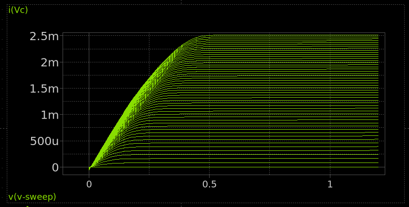
Characteristics curve
The output characteristics of a BJT (i.e., \(I_C\) vs \(V_{CE}\) for different \(I_B\) values) show how the collector current varies with collector-emitter voltage:
IC level Implementation
At the IC level, BJTs are commonly implemented using bipolar processes, such as the BiCMOS (Bipolar CMOS) process, which combines bipolar and CMOS devices on a single chip. In standard bipolar or Bi-CMOS processes, the BJT is built vertically through the silicon substrate. The vertical NPN transistor, which is more common, is constructed with:
- Emitter: A shallow n+ diffusion,
- Base: A p-type region beneath the emitter,
- Collector: A deep n-type region reaching into the substrate.
This vertical structure provides high current density and better performance at high frequencies.
BJTs in ICs are often used for:
- Analog signal amplification,
- Bandgap references,
- High-speed digital drivers,
- Temperature sensors.
Although CMOS has largely replaced BJTs in most digital logic, BJTs remain essential in analog and mixed-signal IC design where precision and speed are critical.
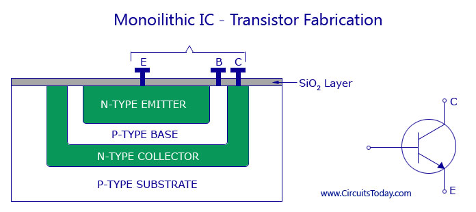
BJT layout
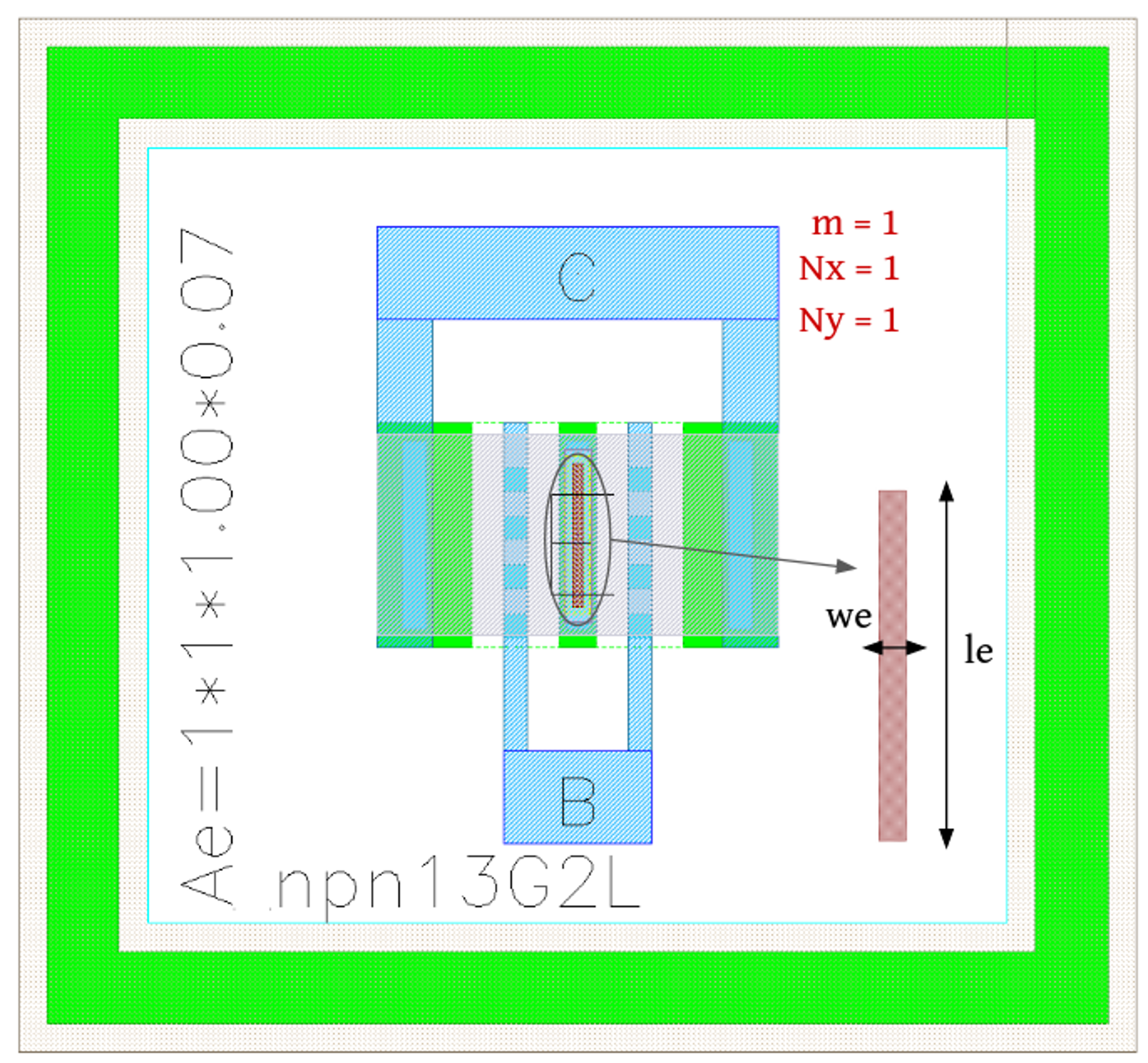
The following image shows a scanned cross section view of a BJT.
