5.1 Design Phase
Table of contents
5.1.1 Background
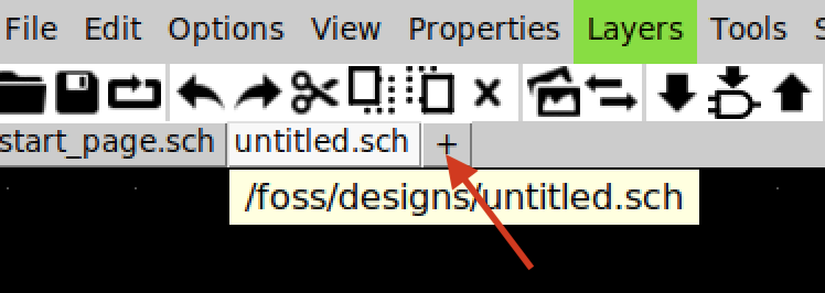
Start by opening the schematic editor Xschem. You can find installation instructions for the IIC OpenSource tools Docker container here.
To begin a new schematic, click the “+” icon.
5.1.2 Component Selection and Placement
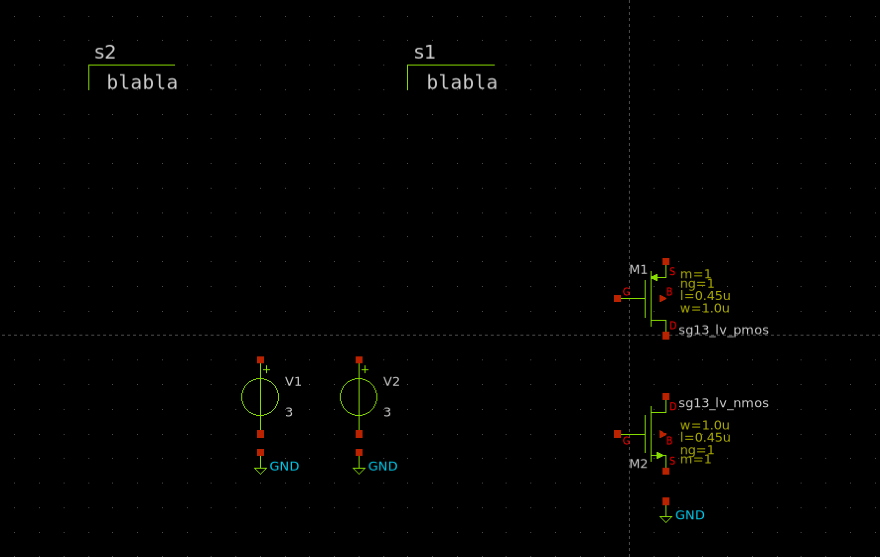
For the inverter circuit, you will need the following components:
- One PMOS transistor
- One NMOS transistor
- Two voltage sources
- Two code_shown components
- Ground pins
To insert these components, navigate to the xschem folder located inside the libs.tech directory of the IHP SG13G2 PDK.
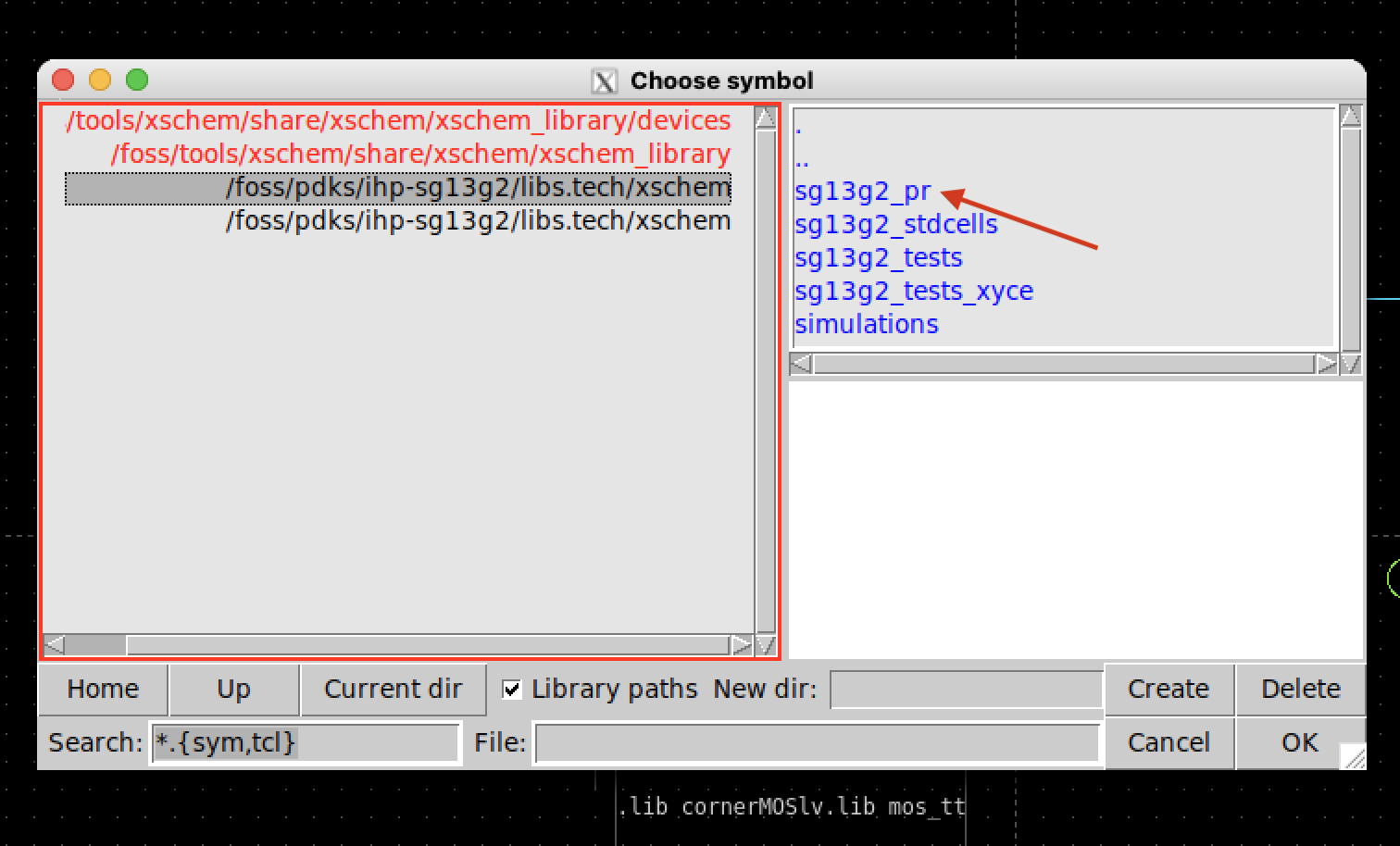
Next, go to the sg13g2_pr directory:

Select the low-voltage MOSFET components:
sg13_lv_pmos.symsg13_lv_nmos.sym
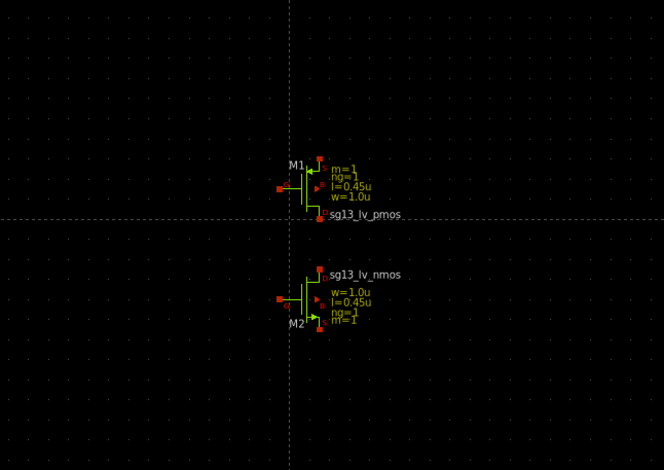
Place these components on the schematic canvas. You can rotate them using Shift + r.
Then, open the devices folder in the xschem_library.
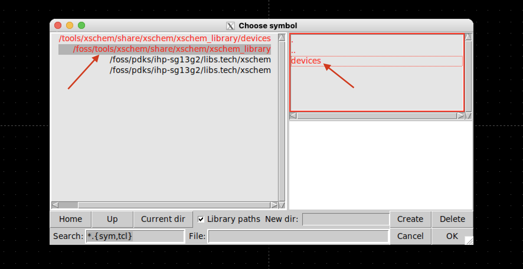
Select the following additional components:
gnd.symvsource.symcode_shown.symlab_pin.sym
Use the “c” key to copy components on the canvas.
The completed component placement should look like this:
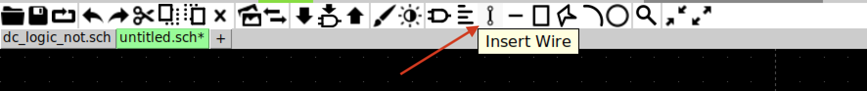
5.1.3 Wiring the Components
Use the “w” key or the wire tool to connect components. To connect nodes without visible wires, you can use lab_pin, which gives a cleaner and more professional layout.
The complete wiring should look like this:
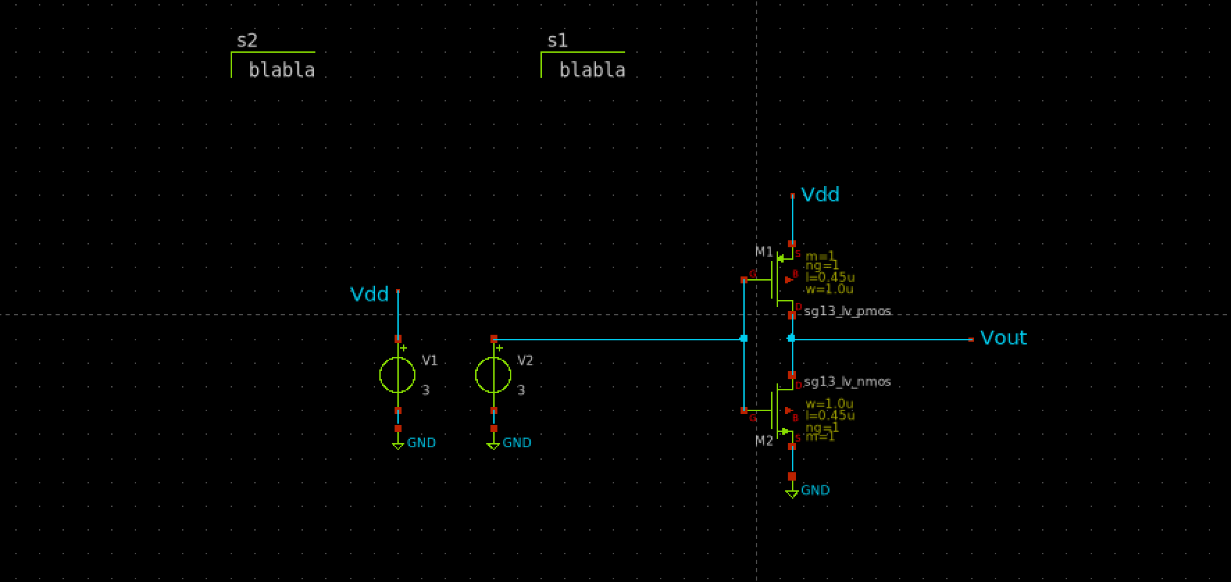
The xschem .sch and .sym files can be found here and here, respectively.
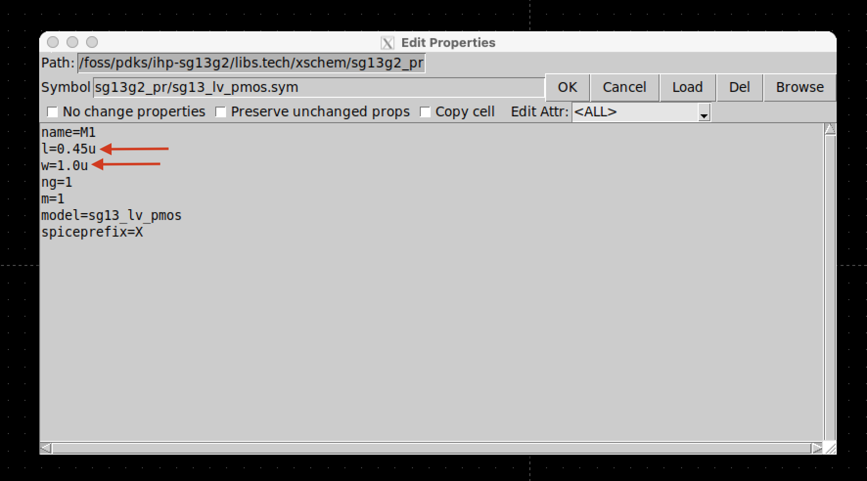
5.1.4 Setting Transistor Parameters
To adjust the W/L ratios of the transistors, double-click on each MOSFET and modify the values in the pop-up window.
Expected Characteristics of a Good Inverter Design:
- Balanced rise and fall times
- Low propagation delay
- Low power consumption
How to choose W/L?
Choose W/L ratios based on the required drive strength and power supply voltage.
You may adjust these parameters after running simulations to meet your specific design goals. For example, increasing the W/L ratio enhances the transconductance (gₘ), which can help reduce delay and increase speed.
For this design:
- PMOS W/L = 20
- NMOS W/L = 10