2.6 The Metal-Oxide-Semiconductor Field-Effect-Transistor (MOSFET)
A Metal-Oxide-Semiconductor Field-Effect Transistor (MOSFET) is a voltage-controlled, four-terminal semiconductor device used to amplify or switch electronic signals. It is the fundamental building block of modern digital and analog integrated circuits. MOSFETs come in two major types: NMOS (n-type) and PMOS (p-type).
Table of Contents
- Characteristics
- Channel Width (W) and Length (L)
- NMOS Transistor
- PMOS Transistor
- 2.5.3 NMOS vs PMOS Comparison
How a MOSFET works
Characteristics
MOSFET operation is controlled by the voltage applied between the gate and source terminals. For an NMOS device, current flows from drain to source when the gate voltage exceeds a certain threshold voltage (\(V_{TH}\)). The current-voltage characteristics can be described by:
- Cut-off Region : MOSFET is OFF.
- Triode (Linear) Region (\(V_{GS} > V_{TH}\) and \(V_{DS} < V_{GS} - V_{TH}\)):
- Saturation Region (\(V_{GS} > V_{TH}\) and \(V_{DS} \ge V_{GS} - V_{TH}\)):
where:
- \(I_D\) is the drain current,
- \(V_{GS}\) is gate-source voltage,
- \(V_{DS}\) is drain-source voltage,
- \(\mu\) = Carrier mobility (electrons for NMOS, holes for PMOS),
- \(C_{ox}\) = Gate oxide capacitance per unit area,
- \(W\) = Channel width,
- \(L\) = Channel length.
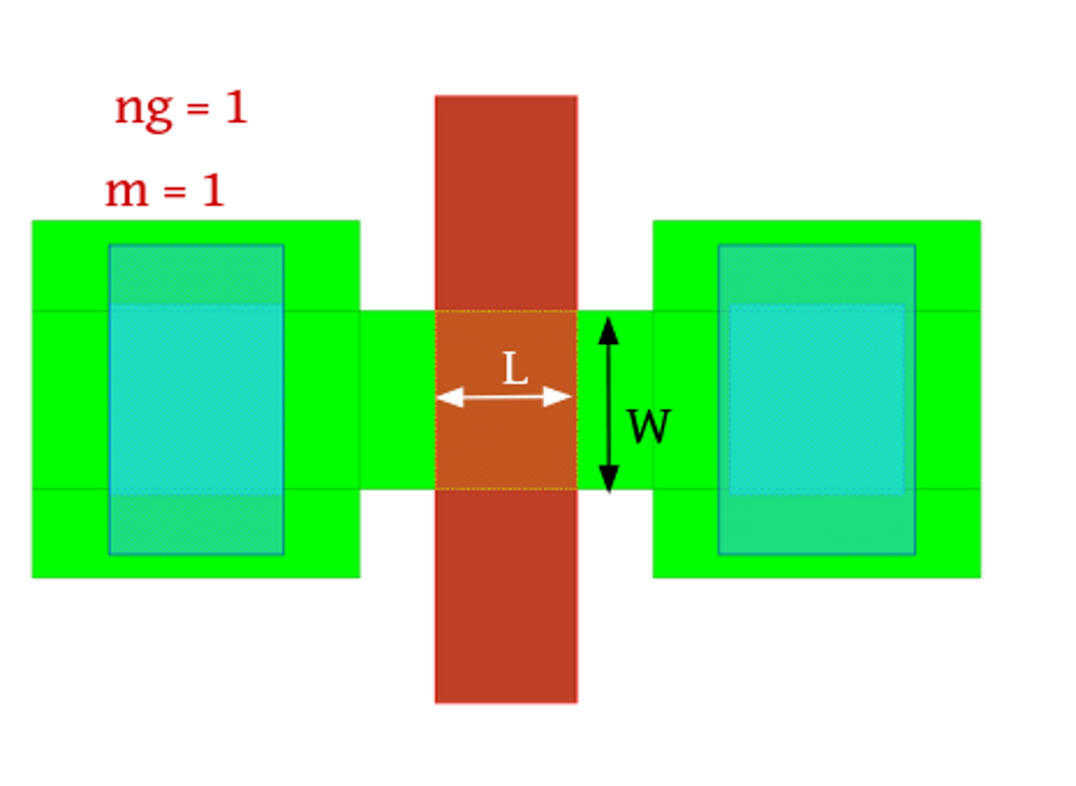
Channel Width (W) and Length (L)
At the IC level, the channel width (W) and channel length (L) of a MOSFET are critical design parameters that directly affect the transistor’s behavior and performance. These dimensions define the size of the channel through which carriers (electrons or holes) flow when the device is on.
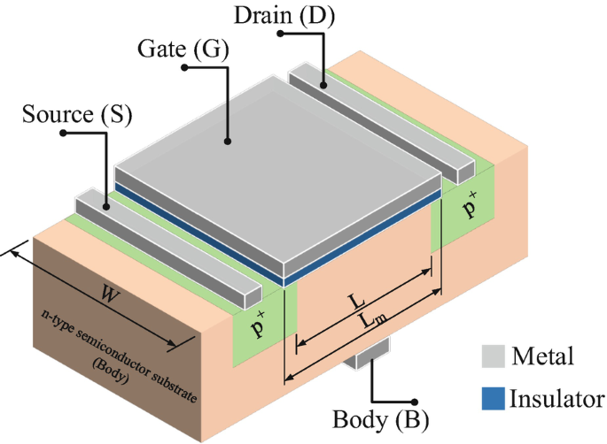
Definitions:
- W (Width): The dimension of the MOSFET channel perpendicular to current flow. A wider channel allows more current.
- L (Length): The dimension of the MOSFET channel along the direction of current flow (distance between source and drain). A shorter length improves speed but increases leakage and short-channel effects.
Impact of W and L:
| Parameter Change | Effect on \(I_D\) | Effect on Speed | Power Impact |
|---|---|---|---|
| Increase W | Increases | Faster drive | Higher dynamic power |
| Increase L | Decreases | Slower | Reduced leakage |
| Decrease L | Increases (shorter path) | Faster switching | Higher leakage |
In digital ICs, minimum L is chosen to maximize speed, while W is adjusted to set the drive strength and balance rise/fall times in CMOS logic gates.
Here is a resource for further understanding of MOSFET physics: UT Dallas.
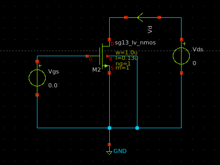
NMOS Transistor
Working Principle
In an NMOS transistor, a positive gate voltage attracts electrons towards the channel, forming a conductive n-type path between the source and drain in a p-type substrate. When \(V_{GS} > V_{TH}\) (threshold voltage), the transistor turns ON, allowing current from drain to source.
Circuit Example
The following schematic shows an NMOS in a common-source configuration:
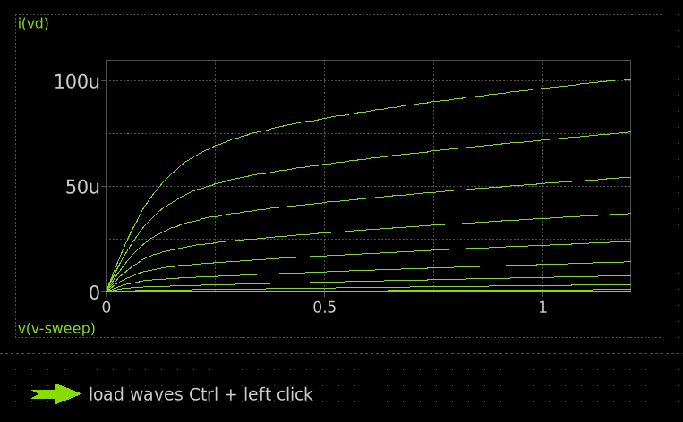
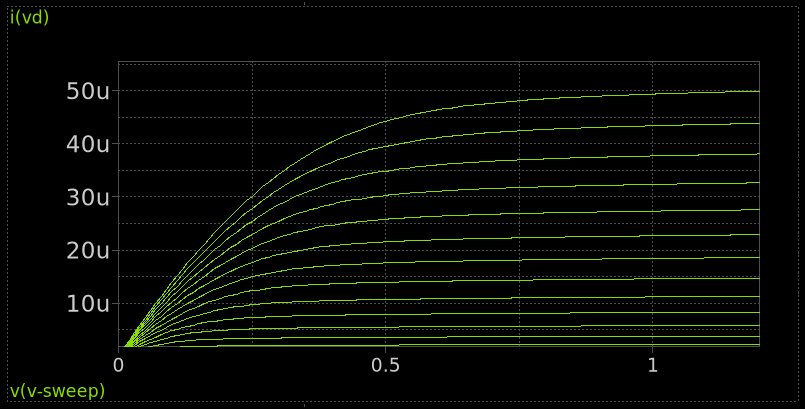
Output Characteristics
The output characteristics (\(I_D\) vs \(V_{DS}\) for different \(V_{GS}\) values) show distinct regions:
- Cut-off: \(V_{GS} < V_{TH}\)
- Triode: \(V_{DS} < V_{GS} - V_{TH}\)
- Saturation: \(V_{DS} \ge V_{GS} - V_{TH}\)
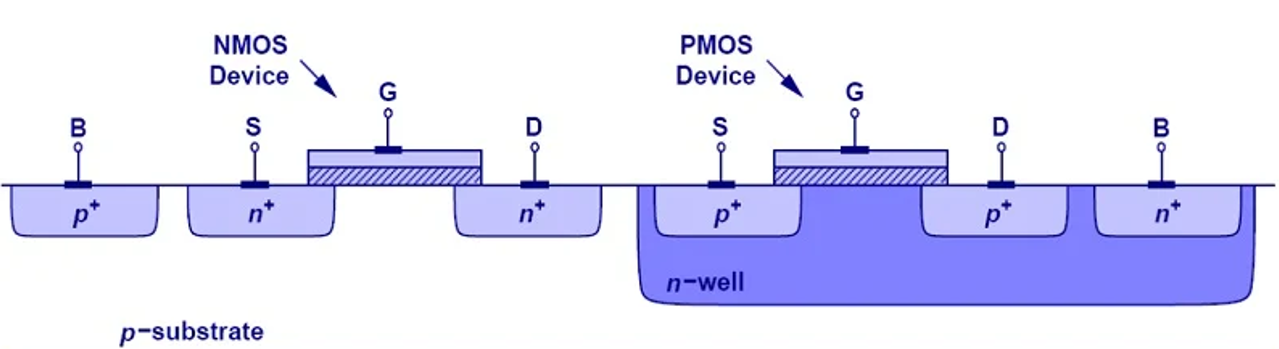
IC-Level Implementation
In ICs, NMOS is fabricated on a p-type substrate, with heavily doped n+ regions for the source and drain, and a polysilicon gate over a thin gate oxide. NMOS devices are typically faster than PMOS due to higher electron mobility.
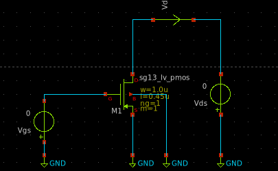
PMOS Transistor
Working Principle
A PMOS transistor operates in the opposite way: a negative gate voltage repels electrons and attracts holes to form a conductive p-type channel in an n-type well. The transistor turns ON when \(V_{SG} > V_{TH}\) (gate is more negative than source).
Circuit Example
The schematic below shows a PMOS transistor in a similar configuration:
Output Characteristics
Similar to NMOS but with reversed voltages and current direction:
- Cut-off: \(V_{SG} < V_{TH}\)
- Triode: \(V_{SD} < V_{SG} - V_{TH}\)
- Saturation: \(V_{SD} \ge V_{SG} - V_{TH}\)
IC-Level Implementation
In CMOS processes, PMOS transistors are fabricated inside an n-well. Source and drain are p+ regions. PMOS devices are typically slower than NMOS due to lower hole mobility, requiring wider channel widths for similar drive strength.
NMOS vs PMOS Comparison
| Feature | NMOS | PMOS |
|---|---|---|
| Channel type | n-type (electrons) | p-type (holes) |
| Substrate | p-type | n-well |
| Conduction when | \(V_{GS} > V_{TH}\) | \(V_{SG} > V_{TH}\) |
| Carrier mobility | Higher (electrons) | Lower (holes) |
| Speed | Faster | Slower |
| Area (for same drive) | Smaller | Larger |
| Symbol direction | Arrow out of source | Arrow into source |
Here is a MOSFET layout design from Magic VLSI.
References
[1] S. P. Gimenez and E. H. S. Galembeck, Differentiated Layout Styles for MOSFETs: Electrical Behavior in Harsh Environments. Cham: Springer International Publishing, 2023. doi: 10.1007/978-3-031-29086-2.
[2] “MOSFET Structure and Operation for Analog IC Design - Technical Articles.” Available: [https://www.allaboutcircuits.com/technical-articles/mosfet-structure-and-operation-for-analog-ic-design/]